
XCKU19P-L1FFVB2104I
XCKU19P-L1FFVB2104I ECAD Model
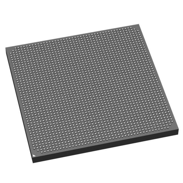
XCKU19P-L1FFVB2104I Attributes
| Type | Description | Select |
|---|---|---|
| Mfr | AMD Xilinx | |
| Series | Virtex® UltraScale+™ | |
| Package | Tray | |
| Number of LABs/CLBs | 105300 | |
| Number of Logic Elements/Cells | 1842750 | |
| Total RAM Bits | 63753421 | |
| Number of I/O | 540 | |
| Voltage - Supply | 0.698V ~ 0.742V | |
| Mounting Type | Surface Mount | |
| Operating Temperature | -40°C ~ 100°C (TJ) | |
| Package / Case | 2104-BBGA, FCBGA | |
| Supplier Device Package | 2104-FCBGA (47.5x47.5) |
XCKU19P-L1FFVB2104I Datasheet Download
XCKU19P-L1FFVB2104I Overview
The XCKU19P-L1FFVB2104I is a Field Programmable Gate Array (FPGA) chip model developed by Xilinx. It is based on the Kintex UltraScale+ architecture and contains a total of 19,200 logic cells, with a maximum operating frequency of 1.3GHz. It also features a total of 1,944 DSP slices, with up to 18x18-bit multipliers and up to 9,728 Kbits of block RAM. Additionally, the chip offers a total of 4,096 I/O pins, with up to 2,560 dedicated to high-speed transceivers.
The chip is designed to provide high-performance data processing capabilities, with its wide range of features and high-speed transceivers. It is suitable for a variety of applications, such as high-speed networking, image and video processing, machine learning, and other data-intensive applications. Additionally, the chip is designed to provide advanced power management capabilities, with a maximum power consumption of up to 11.2W.
In terms of design, the chip is equipped with a wide range of features, including an integrated clock management unit, enhanced DSP slices, and a range of high-speed transceivers. It also supports various memory interfaces, including DDR4, LPDDR4, and QDRII+. Furthermore, the chip is designed to be compatible with a wide range of development tools, such as Vivado Design Suite, Vivado HLS, and System Generator.
Overall, the XCKU19P-L1FFVB2104I is an advanced FPGA chip model designed to provide high-performance data processing capabilities. It is suitable for a wide range of applications and offers advanced power management capabilities. Additionally, the chip is equipped with a wide range of features and is compatible with various development tools.
You May Also Be Interested In

4,200 In Stock
Pricing (USD)
| QTY | Unit Price | Ext Price |
|---|---|---|
| 1+ | $9,527.5800 | $9,527.5800 |
| 10+ | $9,337.0284 | $93,370.2840 |
| 100+ | $9,146.4768 | $914,647.6800 |
| 500+ | $9,051.2010 | $4,525,600.5000 |
| 1000+ | $8,860.6494 | $8,860,649.4000 |
| The price is for reference only, please refer to the actual quotation! | ||