
EP2C15AF484I6
EP2C15AF484I6 ECAD Model
EP2C15AF484I6 Attributes
| Type | Description | Select |
|---|---|---|
| Pbfree Code | No | |
| Rohs Code | No | |
| Part Life Cycle Code | Transferred | |
| Supply Voltage-Nom | 1.2 V | |
| Number of Inputs | 315 | |
| Number of Outputs | 307 | |
| Number of Logic Cells | 14448 | |
| Programmable Logic Type | FIELD PROGRAMMABLE GATE ARRAY | |
| Package Shape | SQUARE | |
| Additional Feature | ALSO REQUIRES 3.3 SUPPLY | |
| Power Supplies | 1.2,1.5/3.3,3.3 V | |
| Supply Voltage-Max | 1.25 V | |
| Supply Voltage-Min | 1.15 V | |
| JESD-30 Code | S-PBGA-B484 | |
| Qualification Status | Not Qualified | |
| JESD-609 Code | e0 | |
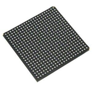
| Number of Terminals | 484 | |
| Package Body Material | PLASTIC/EPOXY | |
| Package Code | BGA | |
| Package Equivalence Code | BGA484,22X22,40 | |
| Package Shape | SQUARE | |
| Package Style | GRID ARRAY | |
| Surface Mount | YES | |
| Terminal Finish | TIN LEAD | |
| Terminal Form | BALL | |
| Terminal Pitch | 1 mm | |
| Terminal Position | BOTTOM | |
| Width | 23 mm | |
| Length | 23 mm | |
| Seated Height-Max | 2.6 mm | |
| Ihs Manufacturer | ALTERA CORP | |
| Part Package Code | BGA | |
| Package Description | FBGA-484 | |
| Pin Count | 484 | |
| Reach Compliance Code | compliant | |
| HTS Code | 8542.39.00.01 |
EP2C15AF484I6 Datasheet Download
EP2C15AF484I6 Overview
The chip model EP2C15AF484I6 is a powerful and versatile integrated circuit (IC) designed for high-performance digital signal processing, embedded processing, and image processing. It is an Altera FPGA device with a wide range of configurations and features, making it an ideal choice for a variety of applications.
The EP2C15AF484I6 is a mid-range device with a maximum operating frequency of 200MHz and a density of up to 4.8 million logic elements. It has 4,832Kbits of embedded SRAM and a variety of peripherals including PLLs, DSP blocks, and high-speed transceivers. In addition, the device has a wide range of I/O options, including LVDS, LVCMOS, and differential I/O standards.
In order to use the EP2C15AF484I6 effectively, it is necessary to have a basic understanding of HDL (Hardware Description Language) programming. The device can be programmed using either Verilog or VHDL, and the user must have a basic understanding of the language and the device’s architecture in order to effectively design and implement a solution.
Case studies of the EP2C15AF484I6 demonstrate its effectiveness in a wide range of applications, including image processing, audio processing, and embedded systems. For example, the device has been used to implement a low-power image processing system for medical imaging. The system was able to process images in real-time and with high accuracy, making it a valuable tool for medical professionals.
When using the EP2C15AF484I6 for any application, it is important to consider the device’s power requirements. The device requires a large amount of power, and it is important to ensure that the power supply is adequate for the application. Additionally, the device should always be operated within the specified temperature and voltage ranges in order to avoid damaging the device.
The EP2C15AF484I6 is a powerful and versatile IC that can be used for a variety of applications. While it is not suitable for the development and popularization of future intelligent robots, it can be used to create powerful embedded systems and image processing solutions. To use the EP2C15AF484I6 effectively, the user must have a basic understanding of HDL programming and must be aware of the device’s power requirements. With the right skills and knowledge, the EP2C15AF484I6 can be used to create powerful and efficient solutions for a variety of applications.
You May Also Be Interested In
1,057 In Stock
Pricing (USD)
| QTY | Unit Price | Ext Price |
|---|---|---|
| No reference price found. | ||