
ICE40LP8K-USBC-EVN
ICE40LP8K-USBC-EVN ECAD Model
ICE40LP8K-USBC-EVN Attributes
| Type | Description | Select |
|---|---|---|
| Mfr | Lattice Semiconductor Corporation | |
| Series | iCE40™ LP | |
| Package | Box | |
| Type | FPGA | |
| For Use With/Related Products | iCE40LP8K | |
| Contents | Board(s) | |
| Base Product Number | ICE40 |
ICE40LP8K-USBC-EVN Datasheet Download
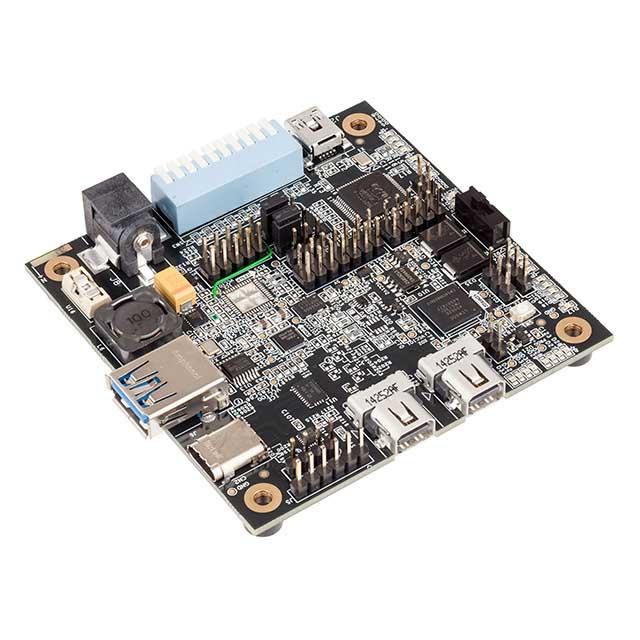
ICE40LP8K-USBC-EVN Overview
The ICE40LP8K-USBC-EVN is an ultra-low power FPGA (Field Programmable Gate Array) chip model developed by Lattice Semiconductor. It is designed to deliver high performance and low power consumption in a wide range of applications.
The ICE40LP8K-USBC-EVN offers 8K logic elements, 256 Kbits of block RAM, and up to 28 dedicated I/O pins. It also includes two general-purpose I/O banks, each with 8 I/O pins. This chip model is compliant with the USB 2.0 standard and supports USB 2.0 full-speed and low-speed communication. It also supports USB On-The-Go (OTG) with integrated PHY, making it suitable for a wide range of applications.
The ICE40LP8K-USBC-EVN is suitable for a wide range of applications, including smart home and building automation, industrial control, medical and healthcare, consumer electronics, automotive, and embedded systems. It can be used to create a variety of designs, including secure data storage, secure communication, and secure authentication.
The ICE40LP8K-USBC-EVN is available in a small, low-profile QFN package, making it ideal for space-constrained applications. It is also RoHS compliant and supports a wide range of operating temperatures, making it suitable for a wide range of applications.
You May Also Be Interested In
4,973 In Stock
Pricing (USD)
| QTY | Unit Price | Ext Price |
|---|---|---|
| No reference price found. | ||