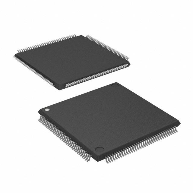

LCMXO2-2000HE-6TG144I
LCMXO2-2000HE-6TG144I ECAD Model
LCMXO2-2000HE-6TG144I Attributes
| Type | Description | Select |
|---|---|---|
| Mfr | Lattice Semiconductor Corporation | |
| Series | MachXO2 | |
| Package | Tray | |
| Number of LABs/CLBs | 264 | |
| Number of Logic Elements/Cells | 2112 | |
| Total RAM Bits | 75776 | |
| Number of I/O | 111 | |
| Voltage - Supply | 1.14V ~ 1.26V | |
| Mounting Type | Surface Mount | |
| Operating Temperature | -40°C ~ 100°C (TJ) | |
| Package / Case | 144-LQFP | |
| Supplier Device Package | 144-TQFP (20x20) | |
| Base Product Number | LCMXO2-2000 |
LCMXO2-2000HE-6TG144I Datasheet Download
LCMXO2-2000HE-6TG144I Overview
The LCMXO2-2000HE-6TG144I is an FPGA chip model manufactured by Lattice Semiconductor. It is based on the LatticeXP2 family of FPGAs and is a high-end device with enhanced features. The chip has 6,144 logic cells, 1,024 Kb of embedded block RAM, and up to 576 I/Os. It also has a wide range of features such as phase-locked loops (PLLs), differential I/Os, and embedded memory. The chip is designed to be used in a wide range of applications, including communications, industrial automation, medical, automotive, and consumer electronics.
The LCMXO2-2000HE-6TG144I has a maximum clock frequency of 200 MHz, and a maximum power consumption of 1.5 W. It also has a wide range of I/O standards such as LVDS, LVCMOS, and SSTL. The chip also has an integrated JTAG and I2C interface, as well as an integrated clock multiplier and divider.
The LCMXO2-2000HE-6TG144I is designed to be used in a wide range of applications, including communications, industrial automation, medical, automotive, and consumer electronics. It can be used in applications such as motor control, robotics, embedded vision, and machine learning. It is also suitable for applications such as networking, security, and storage.
In summary, the LCMXO2-2000HE-6TG144I is a high-end FPGA chip model manufactured by Lattice Semiconductor. It has 6,144 logic cells, 1,024 Kb of embedded block RAM, and up to 576 I/Os. It is designed for use in a wide range of applications, including communications, industrial automation, medical, automotive, and consumer electronics.
You May Also Be Interested In

3,827 In Stock
Pricing (USD)
| QTY | Unit Price | Ext Price |
|---|---|---|
| 1+ | $17.4000 | $17.4000 |
| 10+ | $17.0520 | $170.5200 |
| 100+ | $16.7040 | $1,670.4000 |
| 500+ | $16.5300 | $8,265.0000 |
| 1000+ | $16.1820 | $16,182.0000 |
| The price is for reference only, please refer to the actual quotation! | ||