
LFE2-20SE-6F672I
LFE2-20SE-6F672I ECAD Model
LFE2-20SE-6F672I Attributes
| Type | Description | Select |
|---|---|---|
| Mfr | Lattice Semiconductor Corporation | |
| Series | ECP2 | |
| Package | Tray | |
| Number of LABs/CLBs | 2625 | |
| Number of Logic Elements/Cells | 21000 | |
| Total RAM Bits | 282624 | |
| Number of I/O | 402 | |
| Voltage - Supply | 1.14V ~ 1.26V | |
| Mounting Type | Surface Mount | |
| Operating Temperature | -40°C ~ 100°C (TJ) | |
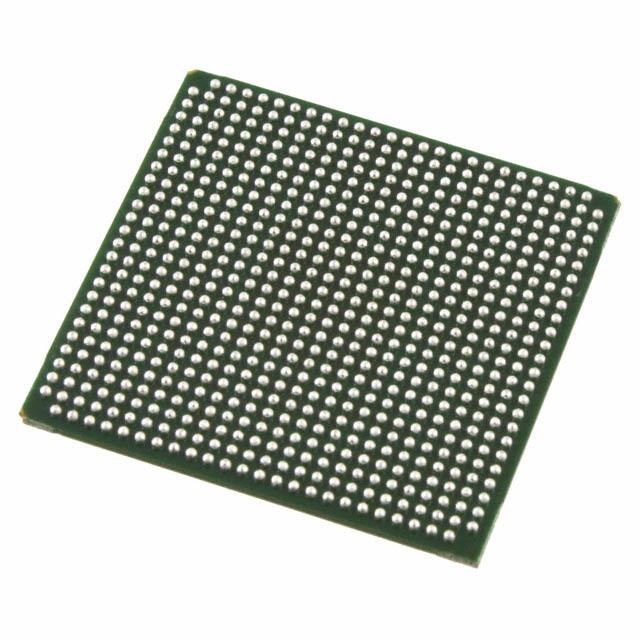
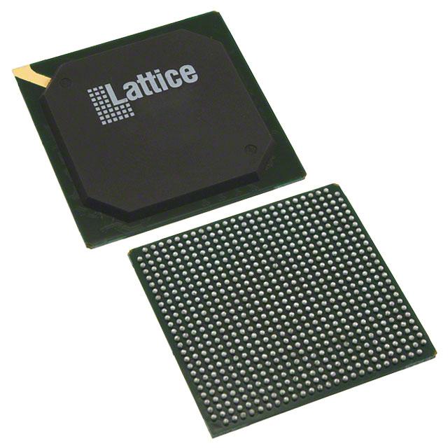
| Package / Case | 672-BBGA | |
| Supplier Device Package | 672-FPBGA (27x27) | |
| Base Product Number | LFE2-20 |
LFE2-20SE-6F672I Datasheet Download
LFE2-20SE-6F672I Overview
The LFE2-20SE-6F672I chip is an FPGA (Field Programmable Gate Array) manufactured by Lattice Semiconductor. It is a low-cost, low-power, high-performance device that is suitable for a range of applications, including digital signal processing (DSP), embedded systems, and communications.
The chip features 6,672 logic elements, 20Kbits of embedded RAM, and up to 6Mbits of on-chip flash memory. It is capable of delivering up to 25 million system gates and up to 50MHz of system performance. It also has built-in phase-locked loops (PLLs), clock multipliers, and on-chip oscillators for increased system performance.
The chip supports a variety of I/O interfaces, including LVDS, LVCMOS, and PCI Express, as well as a wide range of power management features. It can be programmed using the Lattice Diamond software, which provides an intuitive graphical user interface for easy programming.
The LFE2-20SE-6F672I chip is ideal for a range of applications, including industrial automation, medical imaging, data acquisition, and consumer electronics. It is also suitable for use in automotive, aerospace, and military applications. Its low-power, high-performance features make it an ideal choice for embedded systems, where power efficiency and performance are key.
You May Also Be Interested In
2,580 In Stock
Pricing (USD)
| QTY | Unit Price | Ext Price |
|---|---|---|
| No reference price found. | ||