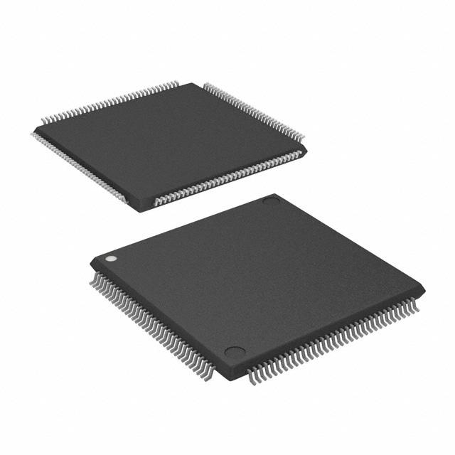

LFE2-6E-5TN144I
LFE2-6E-5TN144I ECAD Model
LFE2-6E-5TN144I Attributes
| Type | Description | Select |
|---|---|---|
| Mfr | Lattice Semiconductor Corporation | |
| Series | ECP2 | |
| Package | Tray | |
| Number of LABs/CLBs | 750 | |
| Number of Logic Elements/Cells | 6000 | |
| Total RAM Bits | 56320 | |
| Number of I/O | 90 | |
| Voltage - Supply | 1.14V ~ 1.26V | |
| Mounting Type | Surface Mount | |
| Operating Temperature | -40°C ~ 100°C (TJ) | |
| Package / Case | 144-LQFP | |
| Supplier Device Package | 144-TQFP (20x20) | |
| Base Product Number | LFE2-6 |
LFE2-6E-5TN144I Datasheet Download
LFE2-6E-5TN144I Overview
The LFE2-6E-5TN144I is an FPGA (Field Programmable Gate Array) chip model produced by the semiconductor manufacturer Lattice Semiconductor. It is a low-cost, low-power, high-performance FPGA device that is suitable for a variety of applications.
The LFE2-6E-5TN144I is built on a 5 nm process technology and is composed of 5.75 million logic cells and 5.75 million embedded memory blocks. It also features 6,000 digital signal processing (DSP) blocks, 16,000 I/O pins, and an up to 500 MHz clock frequency.
The chip model is designed for applications requiring a low power consumption, high speed, and high performance. It is ideal for a variety of applications, including consumer electronics, automotive, industrial, medical, and aerospace. It is also suitable for applications requiring high-speed signal processing, such as video and image processing, as well as embedded systems requiring high-speed data transfer.
The LFE2-6E-5TN144I is also designed to be easy to use and program. It is compatible with a range of software tools, such as the Lattice Diamond design suite and the Lattice Radiant development suite. The chip also features an integrated JTAG programming interface, allowing it to be easily programmed and debugged.
Overall, the LFE2-6E-5TN144I is a powerful, low-cost and low-power FPGA chip model that is suitable for a variety of applications requiring high-speed signal processing and data transfer. It is easy to use and program, and is compatible with a range of software tools.
You May Also Be Interested In

4,818 In Stock
Pricing (USD)
| QTY | Unit Price | Ext Price |
|---|---|---|
| 1+ | $12.3200 | $12.3200 |
| 10+ | $12.0736 | $120.7360 |
| 100+ | $11.7040 | $1,170.4000 |
| 1000+ | $11.4576 | $5,728.8000 |
| 10000+ | $10.9648 | $10,964.8000 |
| The price is for reference only, please refer to the actual quotation! | ||