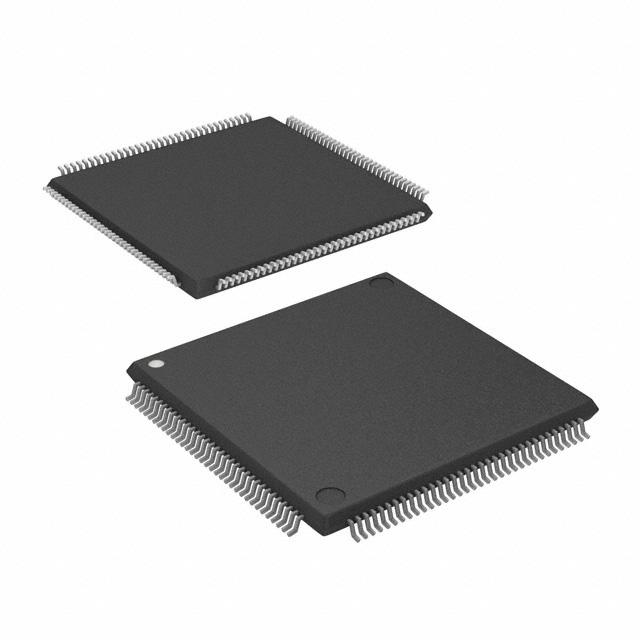

LFEC6E-3T144I
LFEC6E-3T144I ECAD Model
LFEC6E-3T144I Attributes
| Type | Description | Select |
|---|---|---|
| Mfr | Lattice Semiconductor Corporation | |
| Series | EC | |
| Package | Tray | |
| Number of Logic Elements/Cells | 6100 | |
| Total RAM Bits | 94208 | |
| Number of I/O | 97 | |
| Voltage - Supply | 1.14V ~ 1.26V | |
| Mounting Type | Surface Mount | |
| Operating Temperature | -40°C ~ 100°C (TJ) | |
| Package / Case | 144-LQFP | |
| Supplier Device Package | 144-TQFP (20x20) | |
| Base Product Number | LFEC6 |
LFEC6E-3T144I Datasheet Download
LFEC6E-3T144I Overview
The LFEC6E-3T144I chip is a low-power, low-cost, high-performance, field-programmable gate array (FPGA) developed by Lattice Semiconductor. It is based on the Lattice ECP6E architecture and is part of the LatticeECP6E family. The LFEC6E-3T144I chip is based on the 28 nm process technology and offers a wide range of features and benefits.
The LFEC6E-3T144I chip has a total of 144K logic elements and delivers up to 3.2TOPS/W of performance at a power consumption of only 5W. It offers up to 1.2Mbits of embedded memory and up to 8.8Mbits of distributed RAM. The device also offers up to 4,096 I/Os, with up to 4,096 LVDS pairs and up to 1,024 I/Os of multi-gigabit transceivers. The device also features up to 4,096 DSP slices, up to 4,096 MACs, up to 256 PLLs, and up to 512 SERDES lanes.
The LFEC6E-3T144I chip is designed for a wide range of applications, including industrial automation, medical imaging, communications, and machine learning. It is suitable for applications requiring high performance, low power, and low cost. The device is also ideal for applications that require high-speed data transfer, such as 4K/8K video processing, high-speed networking, and machine vision.
In conclusion, the LFEC6E-3T144I chip is a low-power, low-cost, high-performance FPGA that is ideal for a wide range of applications. It offers up to 3.2TOPS/W of performance at a power consumption of only 5W and features up to 4,096 I/Os, up to 4,096 LVDS pairs, up to 1,024 multi-gigabit transceivers, up to 4,096 DSP slices, up to 4,096 MACs, up to 256 PLLs, and up to 512 SERDES lanes.
You May Also Be Interested In

367 In Stock
Pricing (USD)
| QTY | Unit Price | Ext Price |
|---|---|---|
| No reference price found. | ||