

LFECP6E-3Q208C
LFECP6E-3Q208C ECAD Model
LFECP6E-3Q208C Attributes
| Type | Description | Select |
|---|---|---|
| Mfr | Lattice Semiconductor Corporation | |
| Series | ECP | |
| Package | Tray | |
| Number of Logic Elements/Cells | 6100 | |
| Total RAM Bits | 94208 | |
| Number of I/O | 147 | |
| Voltage - Supply | 1.14V ~ 1.26V | |
| Mounting Type | Surface Mount | |
| Operating Temperature | 0°C ~ 85°C (TJ) | |
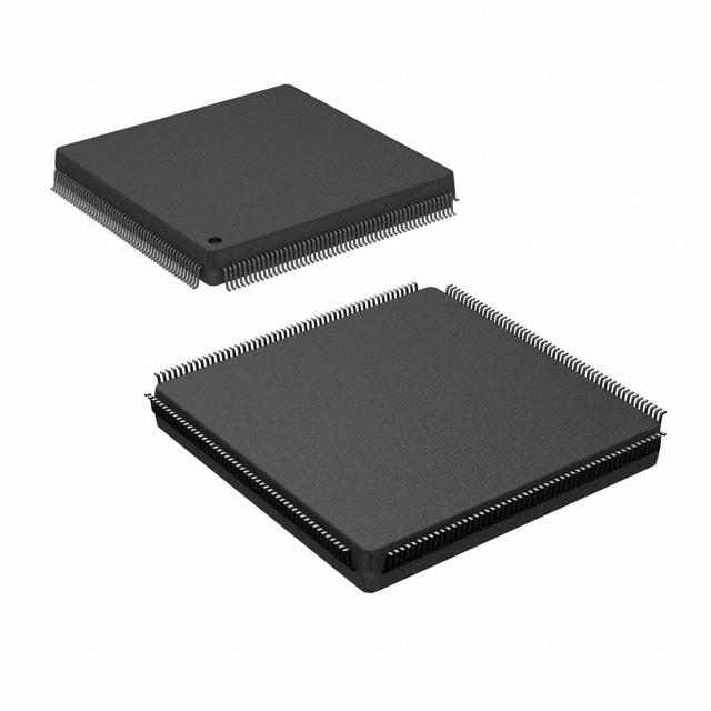
| Package / Case | 208-BFQFP | |
| Supplier Device Package | 208-PQFP (28x28) | |
| Base Product Number | LFECP6 |
LFECP6E-3Q208C Overview
The LFECP6E-3Q208C is a Field Programmable Gate Array (FPGA) chip from Lattice Semiconductor Corporation. It is a low-cost, low-power, high-performance FPGA with a wide range of applications.
The LFECP6E-3Q208C is a 28nm FPGA with a capacity of over 8 million logic elements (LEs). It has a total of 208 I/O pins and a maximum clock frequency of up to 500MHz. The chip is equipped with an embedded memory of up to 6.8Mbits and supports up to 4 independent PLLs. It also supports up to 8 user-configurable banks of DDR3/DDR2/DDR SDRAM.
The LFECP6E-3Q208C is well suited for a variety of applications, including industrial automation, automotive, medical, consumer, and communications. It is ideal for applications that require a low power and low cost solution. The chip also supports a wide range of peripherals and interfaces, including USB, Ethernet, I2C, SPI, and UART.
In conclusion, the LFECP6E-3Q208C is a low-cost, low-power, high-performance FPGA that is suitable for a wide range of applications. It has a capacity of over 8 million logic elements and a maximum clock frequency of up to 500MHz. The chip also supports up to 8 user-configurable banks of DDR3/DDR2/DDR SDRAM and supports a wide range of peripherals and interfaces.
You May Also Be Interested In
1,847 In Stock
Pricing (USD)
| QTY | Unit Price | Ext Price |
|---|---|---|
| No reference price found. | ||