
AGLN060V2-CSG81I
AGLN060V2-CSG81I ECAD Model
AGLN060V2-CSG81I Attributes
| Type | Description | Select |
|---|---|---|
| Rohs Code | Yes | |
| Part Life Cycle Code | Transferred | |
| Supply Voltage-Nom | 1.2 V | |
| Number of Equivalent Gates | 60000 | |
| Number of CLBs | 1536 | |
| Programmable Logic Type | FIELD PROGRAMMABLE GATE ARRAY | |
| Temperature Grade | INDUSTRIAL | |
| Package Shape | SQUARE | |
| Technology | CMOS | |
| Organization | 1536 CLBS, 60000 GATES | |
| Supply Voltage-Max | 1.575 V | |
| Supply Voltage-Min | 1.14 V | |
| JESD-30 Code | S-PBGA-B81 | |
| Qualification Status | Not Qualified | |
| JESD-609 Code | e1 | |
| Moisture Sensitivity Level | 3 | |
| Operating Temperature-Max | 85 °C | |
| Operating Temperature-Min | -40 °C | |
| Peak Reflow Temperature (Cel) | 260 | |
| Time@Peak Reflow Temperature-Max (s) | 30 | |
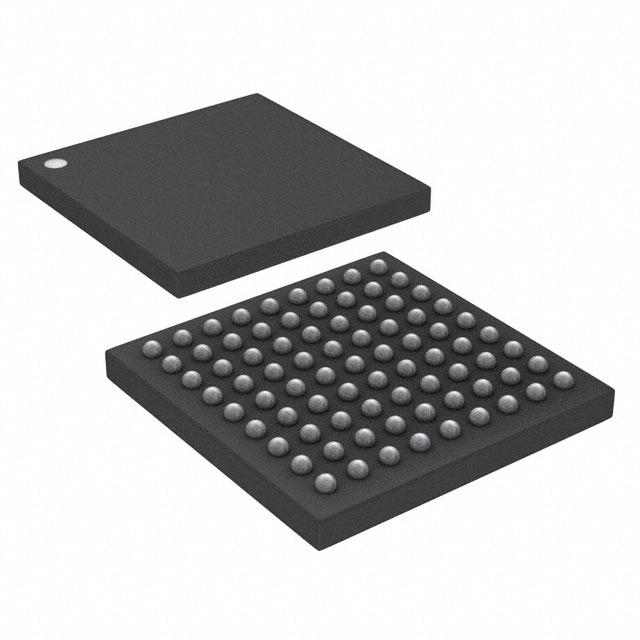
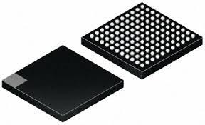
| Number of Terminals | 81 | |
| Package Body Material | PLASTIC/EPOXY | |
| Package Code | VFBGA | |
| Package Shape | SQUARE | |
| Package Style | GRID ARRAY, VERY THIN PROFILE, FINE PITCH | |
| Surface Mount | YES | |
| Terminal Finish | TIN SILVER COPPER | |
| Terminal Form | BALL | |
| Terminal Pitch | 500 µm | |
| Terminal Position | BOTTOM | |
| Width | 5 mm | |
| Length | 5 mm | |
| Seated Height-Max | 800 µm | |
| Ihs Manufacturer | MICROSEMI CORP | |
| Package Description | VFBGA, | |
| Reach Compliance Code | compliant | |
| HTS Code | 8542.39.00.01 |
AGLN060V2-CSG81I Datasheet Download
AGLN060V2-CSG81I Overview
AGLN060V2-CSG81I is a field-programmable gate array (FPGA) chip manufactured by Altera Corporation. It is a mid-range FPGA with a capacity of 60K logic elements, 8,816 Kbits of embedded RAM, and 8,192 Kbits of distributed RAM. It also has a total of 1,024 18-Kbit block RAMs, 1,024 18-Kbit distributed RAMs, and 1,024 18-Kbit distributed ROMs.
The chip has an operating voltage range of 1.2V to 3.3V and a maximum operating temperature range of 0°C to 85°C. It has a total of 8 high-speed serial transceivers, each with a data rate of up to 12.5 Gbps. It also has a total of 8 DSP blocks and 8 clock management tiles. The chip has a total of 8 I/O banks, each with a VCCIO voltage range of 1.2V to 3.3V.
The chip is suitable for a wide range of applications, including high-speed networking, video and image processing, embedded systems, and high-speed signal processing. It is also suitable for applications requiring low power consumption and high reliability. It is also used in automotive, industrial, and medical applications. It has been used in a variety of projects, including the development of a high-speed data acquisition system, a high-speed video processing system, and a high-speed signal processing system.
You May Also Be Interested In
504 In Stock
Pricing (USD)
| QTY | Unit Price | Ext Price |
|---|---|---|
| No reference price found. | ||