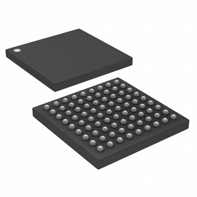

AGLN125V2-CSG81
AGLN125V2-CSG81 ECAD Model
AGLN125V2-CSG81 Attributes
| Type | Description | Select |
|---|---|---|
| Rohs Code | Yes | |
| Part Life Cycle Code | Transferred | |
| Supply Voltage-Nom | 1.2 V | |
| Number of Equivalent Gates | 125000 | |
| Number of CLBs | 3072 | |
| Programmable Logic Type | FIELD PROGRAMMABLE GATE ARRAY | |
| Temperature Grade | OTHER | |
| Package Shape | SQUARE | |
| Technology | CMOS | |
| Organization | 3072 CLBS, 125000 GATES | |
| Supply Voltage-Max | 1.575 V | |
| Supply Voltage-Min | 1.14 V | |
| JESD-30 Code | S-PBGA-B81 | |
| Qualification Status | Not Qualified | |
| Moisture Sensitivity Level | 3 | |
| Operating Temperature-Max | 70 °C | |
| Operating Temperature-Min | -20 °C | |
| Peak Reflow Temperature (Cel) | 260 | |
| Time@Peak Reflow Temperature-Max (s) | 30 | |
| Number of Terminals | 81 | |
| Package Body Material | PLASTIC/EPOXY | |
| Package Code | VFBGA | |
| Package Shape | SQUARE | |
| Package Style | GRID ARRAY, VERY THIN PROFILE, FINE PITCH | |
| Surface Mount | YES | |
| Terminal Form | BALL | |
| Terminal Pitch | 500 µm | |
| Terminal Position | BOTTOM | |
| Width | 5 mm | |
| Length | 5 mm | |
| Seated Height-Max | 800 µm | |
| Ihs Manufacturer | MICROSEMI CORP | |
| Package Description | VFBGA, | |
| Reach Compliance Code | compliant | |
| HTS Code | 8542.39.00.01 |
AGLN125V2-CSG81 Datasheet Download
AGLN125V2-CSG81 Overview
The AGLN125V2-CSG81 is a high-performance, low-power chip model designed for use in a variety of applications. It is a single-channel, 8-bit, 125MHz, low-noise, high-speed analog-to-digital converter (ADC) with a wide dynamic range. The AGLN125V2-CSG81 also features a low-power, low-noise, high-speed, high-resolution, low-distortion, and low-cost design. It is suitable for applications such as medical imaging, industrial automation, automotive, and aerospace.
The AGLN125V2-CSG81 features a sampling rate of up to 125MHz, with a SNR of up to 87dB and a THD of up to -105dB. It has a maximum input voltage of 5V, an input impedance of 50Ω, and a power consumption of 0.5W. The chip also features an integrated temperature sensor, a low-power standby mode, and a programmable gain amplifier (PGA).
The AGLN125V2-CSG81 is designed for a wide range of applications, including medical imaging, industrial automation, automotive, and aerospace. In medical imaging, the AGLN125V2-CSG81 can be used for ultrasound, magnetic resonance imaging (MRI), and computed tomography (CT) scans. In industrial automation, the chip can be used for motor control, robotics, and machine vision. In automotive, the chip can be used for radar, LiDAR, and ADAS systems. In aerospace, the chip can be used for navigation, guidance, and control systems.
Overall, the AGLN125V2-CSG81 is a high-performance, low-power chip model that is suitable for a wide range of applications. It features a high-speed, high-resolution, low-distortion, and low-cost design. Its wide dynamic range, low-power standby mode, and integrated temperature sensor make it a great choice for a variety of applications.
You May Also Be Interested In
929 In Stock
Pricing (USD)
| QTY | Unit Price | Ext Price |
|---|---|---|
| No reference price found. | ||