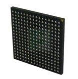

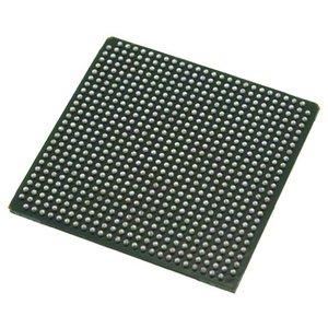
XCS40-4BGG256C
XCS40-4BGG256C ECAD Model
XCS40-4BGG256C Attributes
| Type | Description | Select |
|---|---|---|
| Rohs Code | Yes | |
| Part Life Cycle Code | Obsolete | |
| Supply Voltage-Nom | 5 V | |
| Number of Equivalent Gates | 13000 | |
| Number of CLBs | 784 | |
| Combinatorial Delay of a CLB-Max | 1.2 ns | |
| Programmable Logic Type | FIELD PROGRAMMABLE GATE ARRAY | |
| Temperature Grade | OTHER | |
| Package Shape | SQUARE | |
| Technology | CMOS | |
| Organization | 784 CLBS, 13000 GATES | |
| Additional Feature | MAXIMUM USABLE GATES 40000 | |
| Clock Frequency-Max | 166 MHz | |
| Supply Voltage-Max | 5.25 V | |
| Supply Voltage-Min | 4.75 V | |
| JESD-30 Code | S-PBGA-B256 | |
| Qualification Status | Not Qualified | |
| JESD-609 Code | e1 | |
| Moisture Sensitivity Level | 3 | |
| Operating Temperature-Max | 85 °C | |
| Peak Reflow Temperature (Cel) | 250 | |
| Time@Peak Reflow Temperature-Max (s) | 30 | |
| Number of Terminals | 256 | |
| Package Body Material | PLASTIC/EPOXY | |
| Package Code | BGA | |
| Package Shape | SQUARE | |
| Package Style | GRID ARRAY | |
| Surface Mount | YES | |
| Terminal Finish | TIN SILVER COPPER | |
| Terminal Form | BALL | |
| Terminal Pitch | 1.27 mm | |
| Terminal Position | BOTTOM | |
| Width | 27 mm | |
| Length | 27 mm | |
| Seated Height-Max | 2.55 mm | |
| Ihs Manufacturer | XILINX INC | |
| Part Package Code | BGA | |
| Package Description | BGA, | |
| Pin Count | 256 | |
| Reach Compliance Code | compliant | |
| HTS Code | 8542.39.00.01 |
XCS40-4BGG256C Datasheet Download
XCS40-4BGG256C Overview
The chip model XCS40-4BGG256C is a powerful and reliable integrated circuit designed for high-performance digital signal processing, embedded processing, and image processing. It is an ideal solution for advanced communication systems, and its original design intention was to provide users with a comprehensive and efficient platform for their projects.
The XCS40-4BGG256C chip model is based on a 256-bit architecture and is compatible with the HDL language. It allows users to develop complex digital systems with great flexibility and scalability. The model is capable of supporting up to four logic blocks and provides a wide range of features including high-speed clock management, embedded memory, and advanced communication interfaces.
The product description of the XCS40-4BGG256C chip model includes its size, power consumption, and operating temperature. It also includes its input and output voltage levels, as well as the recommended operating conditions. The product also includes a comprehensive set of design guidelines and requirements, which must be followed in order to ensure the successful implementation of the chip model.
In order to better illustrate the potential of the XCS40-4BGG256C chip model, several case studies have been conducted. These case studies highlight the model’s ability to perform complex tasks with great speed and accuracy. Furthermore, the case studies also provide valuable insights into the model’s performance under various conditions.
When using the XCS40-4BGG256C chip model, it is important to take certain precautions. This includes ensuring that the chip is properly cooled, as well as avoiding any sudden power surges or voltage spikes. Furthermore, users should also ensure that the chip is not exposed to any extreme temperatures or any other environmental hazards.
The XCS40-4BGG256C chip model is a powerful and reliable integrated circuit that is suitable for a wide range of applications. Its original design intention was to provide users with a comprehensive and efficient platform for their projects, and its potential for future upgrades is also quite high. With its wide range of features and capabilities, the XCS40-4BGG256C chip model is an ideal solution for advanced communication systems.
You May Also Be Interested In
3,640 In Stock
Pricing (USD)
| QTY | Unit Price | Ext Price |
|---|---|---|
| No reference price found. | ||