EP20K100FC196-1
EP20K100FC196-1 ECAD Model
EP20K100FC196-1 Attributes
| Type | Description | Select |
|---|---|---|
| Part Life Cycle Code | Obsolete | |
| Supply Voltage-Nom | 2.5 V | |
| Number of Dedicated Inputs | 4 | |
| Programmable Logic Type | LOADABLE PLD | |
| Temperature Grade | OTHER | |
| Package Shape | SQUARE | |
| Organization | 4 DEDICATED INPUTS | |
| Output Function | MACROCELL | |
| Supply Voltage-Max | 2.625 V | |
| Supply Voltage-Min | 2.375 V | |
| JESD-30 Code | S-PBGA-B196 | |
| Qualification Status | Not Qualified | |
| JESD-609 Code | e1 | |
| Operating Temperature-Max | 85 °C | |
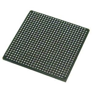
| Number of Terminals | 196 | |
| Package Body Material | PLASTIC/EPOXY | |
| Package Code | BGA | |
| Package Shape | SQUARE | |
| Package Style | GRID ARRAY | |
| Surface Mount | YES | |
| Terminal Finish | TIN SILVER COPPER | |
| Terminal Form | BALL | |
| Terminal Pitch | 1 mm | |
| Terminal Position | BOTTOM | |
| Width | 15 mm | |
| Length | 15 mm | |
| Seated Height-Max | 2.1 mm | |
| Ihs Manufacturer | INTEL CORP | |
| Package Description | BGA, | |
| Reach Compliance Code | compliant | |
| HTS Code | 8542.39.00.01 |
EP20K100FC196-1 Datasheet Download
EP20K100FC196-1 Overview
The chip model EP20K100FC196-1 is a powerful integrated circuit designed for high-performance digital signal processing, embedded processing, and image processing. It is based on a Field Programmable Gate Array (FPGA) architecture, and requires the use of HDL (Hardware Description Language) for programming. This makes it an ideal candidate for applications where complex algorithms need to be implemented in a cost-effective manner.
The EP20K100FC196-1 is designed to provide a high-performance, low-power solution for digital signal processing applications. It is capable of operating at frequencies up to 200MHz, and can be configured to support multiple clock domains. This makes it suitable for applications such as advanced communication systems, where multiple clock domains are needed for efficient operation.
The EP20K100FC196-1 has an array of features that make it suitable for a wide range of applications. It has a large number of programmable logic blocks, which can be used to implement complex algorithms. It also supports multiple I/O standards, including LVDS, SSTL, and LVCMOS, making it suitable for a variety of applications. Additionally, it supports on-chip memory, which can be used for data storage and manipulation.
The EP20K100FC196-1 is designed to be upgradable in the future. It can be configured to support additional clock domains and different I/O standards, allowing it to be used for more complex applications. Additionally, its programmable logic blocks can be reconfigured to support new algorithms, making it suitable for a wide range of applications.
In order to ensure that the EP20K100FC196-1 is used correctly, it is important to understand its design requirements. It is important to ensure that the correct HDL language is used, and that the correct I/O standards are supported. Additionally, it is important to ensure that the correct clock domains are configured, and that the correct memory configuration is used.
The EP20K100FC196-1 has been used in a variety of applications, ranging from image processing to advanced communication systems. In all cases, it has proven to be a reliable and cost-effective solution for complex digital signal processing applications. By understanding its design requirements and capabilities, users can ensure that they are able to get the most out of this powerful integrated circuit.
You May Also Be Interested In
1,148 In Stock
Pricing (USD)
| QTY | Unit Price | Ext Price |
|---|---|---|
| No reference price found. | ||


