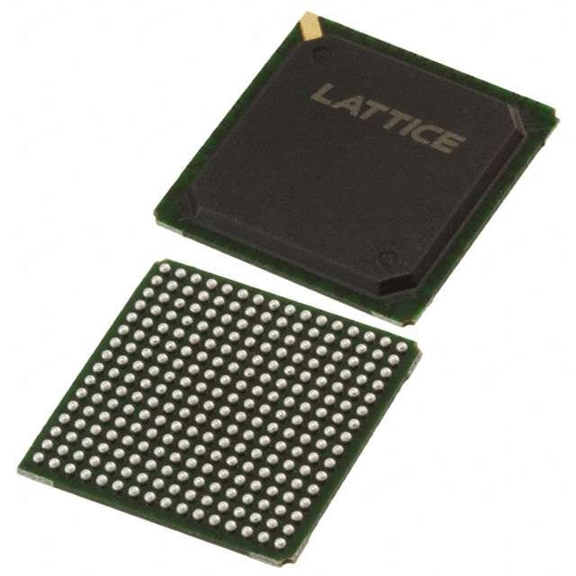

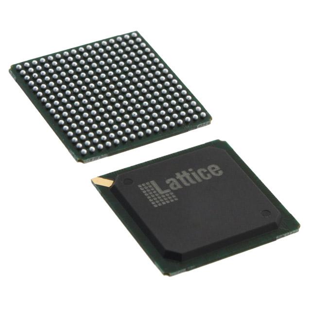
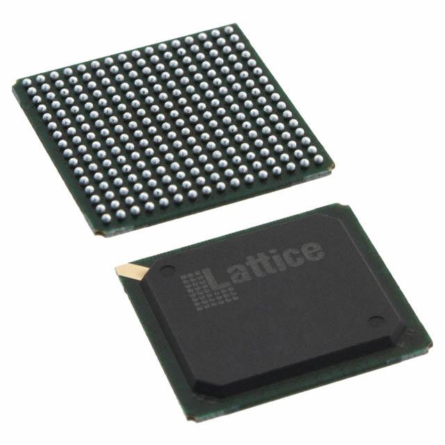
LC5256MB-5F256I
LC5256MB-5F256I ECAD Model
LC5256MB-5F256I Attributes
| Type | Description | Select |
|---|---|---|
| Mfr | Lattice Semiconductor Corporation | |
| Series | ispXPLD® 5000MB | |
| Package | Tray | |
| Programmable Type | In System Programmable | |
| Delay Time tpd(1) Max | 5 ns | |
| Voltage Supply - Internal | 2.3V ~ 2.7V | |
| Number of Logic Elements/Blocks | 8 | |
| Number of Macrocells | 256 | |
| Number of I/O | 141 | |
| Operating Temperature | -40°C ~ 105°C (TJ) | |
| Mounting Type | Surface Mount | |
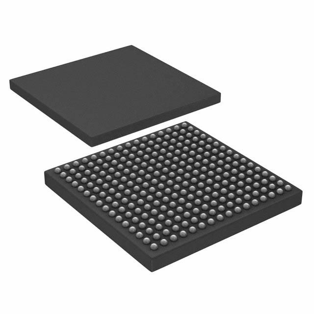
| Package / Case | 256-BGA | |
| Supplier Device Package | 256-FPBGA (17x17) | |
| Base Product Number | LC5256 |
LC5256MB-5F256I Datasheet Download
LC5256MB-5F256I Overview
The LC5256MB-5F256I is a high-performance, low-power FPGA chip designed by Lattice Semiconductor. It is a member of the MachXO2 family and is the first FPGA to be offered in a BGA package. The device is based on the LatticeECP2M architecture and features 5,256 logic cells, 256 Kbits of embedded memory, and a wide range of I/O options. It is ideal for applications requiring a combination of high performance, low power consumption, and small form factor.
The LC5256MB-5F256I has a total of 5,256 logic cells, 256 Kbits of embedded memory, and up to 456 I/O pins. It is capable of up to 500 MHz operation and features low power consumption of just 1.2 W. The device also includes a range of advanced features such as low-skew clock networks, dedicated high-speed I/O, and an integrated PCIe Gen2 x4 interface.
The LC5256MB-5F256I is suitable for a wide range of applications, including industrial automation, medical imaging, and consumer electronics. It is also well suited for use in high-speed networking, communications, and video applications. The device is available in a BGA package, which makes it easy to integrate into existing designs and provides a high level of flexibility.
In summary, the LC5256MB-5F256I is a high-performance, low-power FPGA chip designed by Lattice Semiconductor. It features 5,256 logic cells, 256 Kbits of embedded memory, and up to 456 I/O pins. It is suitable for a wide range of applications, including industrial automation, medical imaging, and consumer electronics. The device is available in a BGA package, which makes it easy to integrate into existing designs and provides a high level of flexibility.
You May Also Be Interested In
1,700 In Stock
Pricing (USD)
| QTY | Unit Price | Ext Price |
|---|---|---|
| No reference price found. | ||