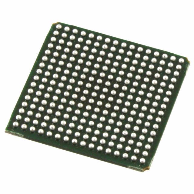

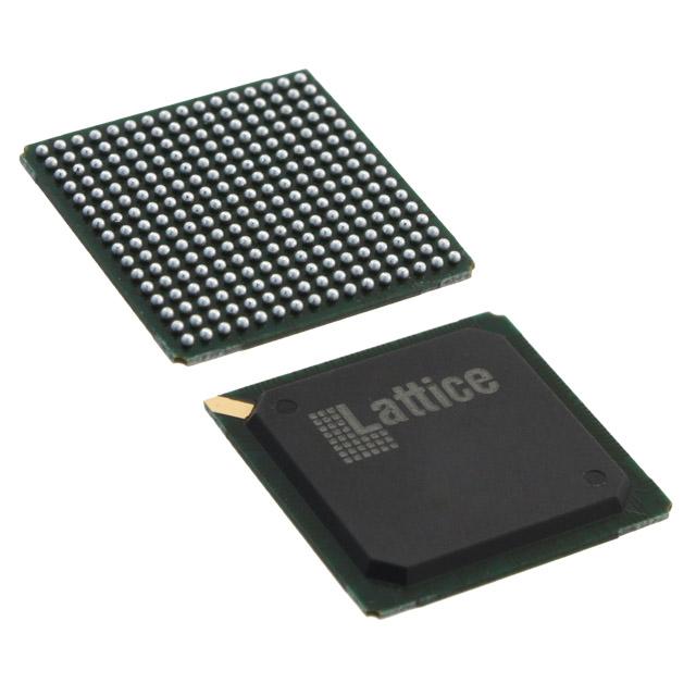
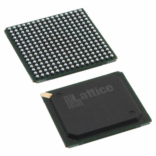
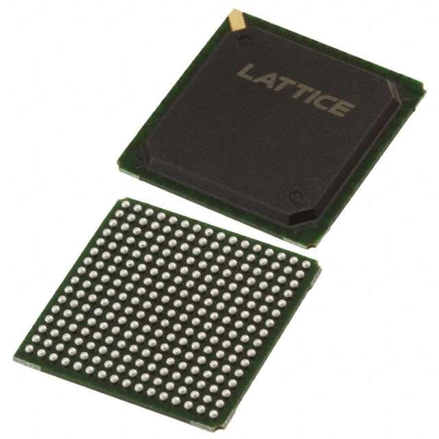
LFX125EB-05F256C
LFX125EB-05F256C ECAD Model
LFX125EB-05F256C Attributes
| Type | Description | Select |
|---|---|---|
| Mfr | Lattice Semiconductor Corporation | |
| Series | ispXPGA® | |
| Package | Tray | |
| Number of Logic Elements/Cells | 1936 | |
| Total RAM Bits | 94208 | |
| Number of I/O | 160 | |
| Number of Gates | 139000 | |
| Voltage - Supply | 2.3V ~ 3.6V | |
| Mounting Type | Surface Mount | |
| Operating Temperature | 0°C ~ 85°C (TJ) | |
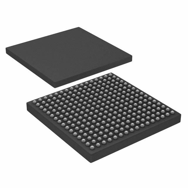
| Package / Case | 256-BGA | |
| Supplier Device Package | 256-FPBGA (17x17) | |
| Base Product Number | LFX125 |
LFX125EB-05F256C Datasheet Download
LFX125EB-05F256C Overview
The LFX125EB-05F256C is a low-power, low-cost, low-voltage, low-power FPGA chip model developed by Lattice Semiconductor. It is based on the Lattice's low-power, low-cost, low-voltage FPGA architecture, and is designed for applications that require low power consumption and cost-effectiveness.
The LFX125EB-05F256C chip model has a total of 256 configurable logic blocks (CLBs), which are organized into four columns and 64 rows. It also has four dedicated DSP blocks, eight dedicated I/O blocks, and four dedicated RAM blocks. The chip model has a total of 4,096 I/O pins and can support up to 8,192 user-defined logic functions. It has an operating voltage range of 1.2V to 3.3V, with a maximum current draw of 1.5A.
The LFX125EB-05F256C chip model is ideal for applications such as automotive, industrial, and medical systems, as well as consumer electronics. It provides a cost-effective solution for applications that require low power consumption, such as portable devices, remote sensors, and wearable electronics. Additionally, it can be used in applications that require high data throughput, such as high-speed communications and networking, as well as image and video processing.
You May Also Be Interested In
4,200 In Stock
Pricing (USD)
| QTY | Unit Price | Ext Price |
|---|---|---|
| No reference price found. | ||