
LX256EV-5F484C
LX256EV-5F484C ECAD Model
LX256EV-5F484C Attributes
| Type | Description | Select |
|---|---|---|
| Mfr | Lattice Semiconductor Corporation | |
| Series | ispGDX2™ | |
| Package | Tray | |
| Number of I/O | 256 | |
| Voltage - Supply | 3V ~ 3.6V | |
| Mounting Type | Surface Mount | |
| Operating Temperature | 0°C ~ 90°C (TJ) | |
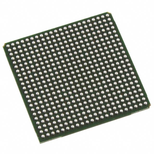
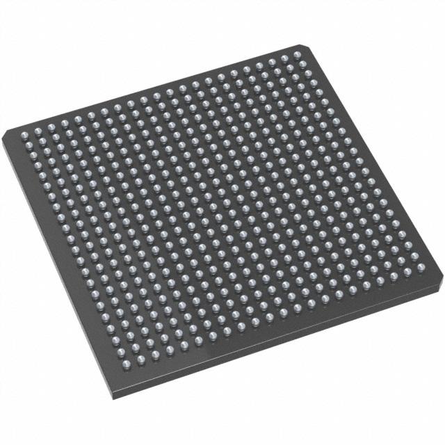
| Package / Case | 484-BBGA | |
| Supplier Device Package | 484-FPBGA (23x23) | |
| Base Product Number | LX256 |
LX256EV-5F484C Datasheet Download
LX256EV-5F484C Overview
The LX256EV-5F484C is a Field Programmable Gate Array (FPGA) chip model manufactured by Lattice Semiconductor. It is based on the LatticeXP2-5 FPGA architecture and is a low-power, low-cost, high-performance device. The LX256EV-5F484C features a total of 256 logic cells, 8 DSP blocks, 4,096 bits of RAM, and 4,096 bits of ROM. It also has 48 I/O pins, 4 global clock inputs, and 2 dedicated clock outputs. The chip operates at a maximum clock frequency of 250 MHz and is designed to operate at a maximum temperature of 105°C.
The LX256EV-5F484C is ideal for a wide range of applications, such as embedded systems, automotive, consumer electronics, industrial control, medical, and aerospace. It is suitable for applications that require low-power, high-performance, and low-cost solutions. It can be used for digital signal processing, image processing, and data acquisition. The device is also suitable for applications that require rapid prototyping, such as prototyping of consumer electronics products.
The LX256EV-5F484C is a highly integrated device that offers a wide range of features and benefits. It is easy to program, has low power consumption, and is highly reliable. It is also easy to integrate into existing systems and can be used in a variety of applications. The device is also RoHS compliant and is available in a variety of packages.
You May Also Be Interested In
2,000 In Stock
Pricing (USD)
| QTY | Unit Price | Ext Price |
|---|---|---|
| No reference price found. | ||