
XC2V40-4FG256I
XC2V40-4FG256I ECAD Model
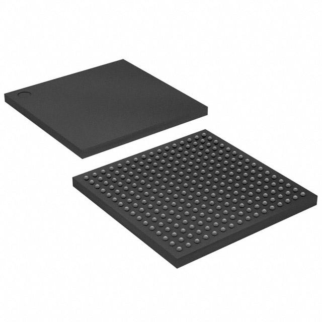
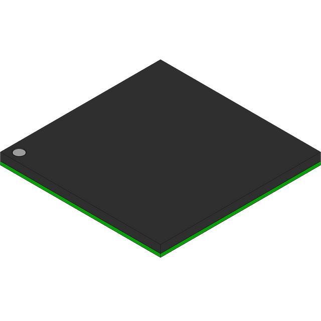
XC2V40-4FG256I Attributes
| Type | Description | Select |
|---|---|---|
| Mfr | AMD Xilinx | |
| Series | Virtex®-II | |
| Package | Tray | |
| Number of LABs/CLBs | 64 | |
| Total RAM Bits | 73728 | |
| Number of I/O | 88 | |
| Number of Gates | 40000 | |
| Voltage - Supply | 1.425V ~ 1.575V | |
| Mounting Type | Surface Mount | |
| Operating Temperature | -40°C ~ 100°C (TJ) | |
| Package / Case | 256-BGA | |
| Supplier Device Package | 256-FBGA (17x17) | |
| Base Product Number | XC2V40 |
XC2V40-4FG256I Datasheet Download
XC2V40-4FG256I Overview
The XC2V40-4FG256I is a Field Programmable Gate Array (FPGA) chip from Xilinx Corporation. It is a member of the Virtex-II Pro family of FPGAs and is based on the Virtex-II Pro platform. It is a high-performance, low-power device with a maximum operating frequency of 200 MHz.
The XC2V40-4FG256I is a 4-layer FPGA that can be used for various applications including digital signal processing, embedded control, and communications. It has 256 macrocells, 4 clock management tiles, and 4 input/output (I/O) blocks. It also features 4-bit lookup tables (LUTs), 4-bit flip-flops, and 4-bit distributed RAMs.
The XC2V40-4FG256I has a total of 256 I/Os, which can be configured as either single-ended or differential. It supports a wide range of I/O standards, including LVTTL, LVCMOS, SSTL2, HSTL, and GTL. It also supports multiplexed I/O, clock-forwarding, and clock-skew management.
The XC2V40-4FG256I is a powerful and versatile FPGA that can be used for a variety of applications, such as digital signal processing, embedded control, and communications. It is ideal for high-performance, low-power applications and can be used in a wide range of industries, including automotive, aerospace, industrial, and medical.
You May Also Be Interested In
3,295 In Stock
Pricing (USD)
| QTY | Unit Price | Ext Price |
|---|---|---|
| No reference price found. | ||