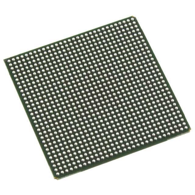

LFE2M100E-5F900I
LFE2M100E-5F900I ECAD Model
LFE2M100E-5F900I Attributes
| Type | Description | Select |
|---|---|---|
| Mfr | Lattice Semiconductor Corporation | |
| Series | ECP2M | |
| Package | Tray | |
| Number of LABs/CLBs | 11875 | |
| Number of Logic Elements/Cells | 95000 | |
| Total RAM Bits | 5435392 | |
| Number of I/O | 416 | |
| Voltage - Supply | 1.14V ~ 1.26V | |
| Mounting Type | Surface Mount | |
| Operating Temperature | -40°C ~ 100°C (TJ) | |
| Package / Case | 900-BBGA | |
| Supplier Device Package | 900-FPBGA (31x31) | |
| Base Product Number | LFE2M100 |
LFE2M100E-5F900I Datasheet Download
LFE2M100E-5F900I Overview
The LFE2M100E-5F900I is a low-power, low-cost, low-power field-programmable gate array (FPGA) chip. It is manufactured by Lattice Semiconductor and is part of the MachXO2 family of FPGA chips. The LFE2M100E-5F900I is a small, low-cost FPGA chip that is ideal for applications requiring low power consumption and cost-effectiveness. It features a maximum power consumption of only 1.2W and a maximum operating temperature of 85°C.
The LFE2M100E-5F900I has a total of 100K logic elements, which includes up to 4,096 logic cells and up to 1,536 flip-flops. It also has up to 4,096 programmable I/O pins and up to 4,096 programmable interconnects. In addition, the chip also has up to 4,096 configurable logic blocks, up to 4,096 configurable memory blocks, up to 4,096 configurable DSP blocks, and up to 4,096 configurable logic blocks.
The LFE2M100E-5F900I chip is suitable for use in a variety of applications, including consumer electronics, industrial automation, medical devices, automotive systems, and more. It is also suitable for use in embedded systems and in applications that require low power consumption and cost-effectiveness. It is also suitable for applications that require high speed, low latency, and high reliability.
In conclusion, the LFE2M100E-5F900I is a low-power, low-cost, low-power FPGA chip that is suitable for use in a variety of applications. It features a maximum power consumption of only 1.2W and a maximum operating temperature of 85°C. It has up to 4,096 logic cells, up to 1,536 flip-flops, up to 4,096 programmable I/O pins, up to 4,096 programmable interconnects, up to 4,096 configurable logic blocks, up to 4,096 configurable memory blocks, up to 4,096 configurable DSP blocks, and up to 4,096 configurable logic blocks. It is suitable for use in applications that require low power consumption and cost-effectiveness, as well as high speed, low latency, and high reliability.
You May Also Be Interested In
4,668 In Stock
Pricing (USD)
| QTY | Unit Price | Ext Price |
|---|---|---|
| No reference price found. | ||